Celeron
The Celeron processor is a chameleon. It was originally a P6 with the same processor core as the Pentium II in the original two versions; later it came with the same core as the PIII; and more recently it uses the Pentium 4 core. It is designed mainly for lower-cost PCs.
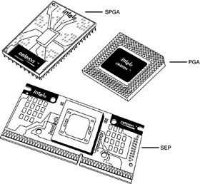
Most of the features for the Celeron are the same as the Pentium II, III, or 4 because it uses the same internal processor cores. The main differences are in packaging, L2 cache amount, and CPU bus speed. The first version of the Celeron was available in a package called the single edge processor package (SEPP or SEP package).
The SEP package is basically the same Slot 1 design as the SECC used in the Pentium II/III, with the exception of the fancy plastic cartridge cover. This cover is deleted in the Celeron, making it cheaper to produce and sell. Essentially, the original Celeron used the same circuit board as is inside the Pentium II package.
Even without the plastic covers, the Slot 1 packaging was more expensive than it should have been. This was largely due to the processor retention mechanisms (stands) required to secure the processor into Slot 1 on the motherboard, as well as the larger and more complicated heatsinks required.
This, plus competition from the lower-end Socket 7 systems using primarily AMD processors, led Intel to introduce the Celeron in a socketed form. The socket is called PGA-370 or Socket 370 because it has 370 pins. The processor package designed for this socket is called the plastic pin grid array (PPGA) package or flip chip PGA (FC-PGA).
Both the PPGA and FC-PGA packages plug into the 370 pin socket and allow for lower-cost, lower-profile, and smaller systems because of the less expensive processor retention and cooling requirements of the socketed processor. All Celeron processors at 433MHz and lower have been available in the SEPP that plugs into the 242-contact slot connector (Slot 1).
The 300MHz and higher versions also are available in the PPGA package. This means that the 300MHz to 433MHz have been available in both packages, whereas the 466MHz and higher-speed versions are available only in the PPGA. The fastest Celeron processor for Socket 370 runs at 1.4GHz; faster Celerons use Socket 478 and are based on the Pentium 4 design.
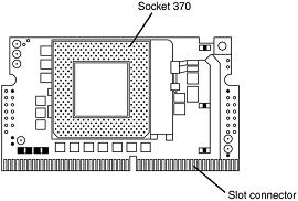
Motherboards that include Socket 370 can accept the PGA versions of both the Celeron and Pentium III in most cases. If you want to use a Socket 370 version of the Celeron in a Slot 1 motherboard, slot-to-socket adapters (usually called slot-kets) are available for about $10–$20 that plug into Slot 1 and incorporate a Socket 370 on the card. Figure below shows a typical slot-ket adapter.
Highlights of the Celeron include the following:
-
Available at 300MHz (300A) and higher core frequencies with 128KB on-die L2 cache; 300MHz and 266MHz core frequencies without L2 cache
-
L2 cache supports up to 4GB RAM address range and ECC
-
Uses same P6 core processor as the Pentium II (266MHz through 533MHz) and now the Pentium III (533A MHz and higher) and Pentium 4 (1.7GHz and higher)
-
Dynamic execution microarchitecture
-
Operates on a 66MHz, 100MHz, or 400MHz CPU bus depending on the version
-
Specifically designed for lower-cost value PC systems
-
Includes MMX technology; Celeron 533A and higher include SSE; Celeron 1.7GHz and higher include SSE2
-
More cost-effective packaging technology, including SEP, PPGA, FC-PGA or FC-PGA2 packages
-
Integrated L1 and L2 cache on most models, with amount and type depending on the version; typically, the Celeron has half the L2 cache of the processor core it is patterned after
-
Integrated thermal diode for temperature monitoring
The Intel Celeron processors from the 300A and higher include integrated 128KB L2 cache. The core for the 300A through 533MHz versions that are based on the Pentium II core include 19 million transistors because of the addition of the integrated 128KB L2 cache.
The 533A and faster versions are based on the Pentium III core and incorporate 28.1 million transistors. The 1.7GHz and faster versions are based on the Pentium 4 core with 42 million transistors. The Pentium III and Pentium 4–based versions actually have 256KB of L2 cache on the die.
However, 128KB is disabled, leaving 128KB of functional L2 cache. This was done because it was cheaper for Intel to simply make the Celeron using the same die as the Pentium III or 4 and just disable part of the cache on the Celeron versions, rather than coming up with a unique die for the newer Celerons.
The Pentium III–based Celeron processors also support the SSE in addition to MMX instructions, whereas the Pentium 4–based versions support SSE2 instructions. The older Celerons based on the Pentium II core support only MMX.
All the Celerons in SEPP and PPGA form are manufactured using the 0.25-micron process, whereas those in FC-PGA and FC-PGA2 form are made using an even better 0.18-micron process. The smaller process reduces processor heat and enables higher speeds.


