Intel 810, 810E, and 810E2 Chipset
Introduced in April 1999, the Intel 810 chipset (code named Whitney) represents a major change in chipset design from the standard North and South Bridges that have been used since the 486 days. The 810 chipset allows for improvements in system performance, all for less cost and system complexity.
The 810 (which supports 66MHz and 100MHz processor buses) was later revised as the 810E with support for the 133MHz processor bus. The major features of the 810E chipset include:
-
66/100/133MHz system bus
-
Integrated AGP 2x Intel 3D graphics
-
Efficient use of system memory for graphics performance
-
Optional 4MB of dedicated display cache video memory
-
Digital Video Out port compatible with DVI specification for flat-panel displays
-
Software MPEG-2 DVD playback with hardware motion compensation
-
266MBps hub interface
-
Support for ATA-66
-
Integrated Audio-Codec 97 (AC'97) controller
-
Support for low-power sleep modes
-
Random number generator (RNG)
-
Integrated USB controller
-
LPC bus for Super I/O and Firmware Hub (ROM BIOS) connection
-
Elimination of ISA bus
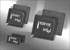
The 810E chipset consists of three major components:
-
82810E Graphics Memory Controller Hub (GMCH). 421 BGA package (the original 810 chipset used the 82810 GMCH).
-
82801 Integrated Controller Hub (ICH). 241 BGA package.
-
82802 Firmware Hub (FWH). In either 32-pin plastic leaded chip carrier (PLCC) or 40-pin thin small outline package (TSOP) packages. Although a functional part of the chipset, this component is actually sold separately by Intel to motherboard developers.
Compared to the previous North/South Bridge designs, there are some fairly significant changes in the 810 chipset. The previous system designs had the North Bridge acting as the memory controller, talking to the South Bridge chip via the PCI bus.
This new design has the GMCH taking the place of the North Bridge, which talks to the ICH via a 66MHz dedicated interface called the accelerated hub architecture (AHA) bus instead of the previously used PCI bus.
In particular, implementing a direct connection between the North and South Bridges in this manner was key in implementing the new UDMA-66 high-speed IDE interface for hard disks, DVD drives, and other IDE devices. The 82810E GMCH uses an internal Direct AGP (integrated AGP) interface to create 2D and 3D effects and images.
The video capability integrated into the 82810E chip features hardware motion compensation to improve software DVD video quality; it also features both analog and direct digital video out ports, which enable connections to either traditional TVs (via an external converter module) or a direct digital flat panel display.
The GMCH chip also incorporates the System Manageability Bus, which enables networking equipment to monitor the 810 chipset platform. Using ACPI specifications, the system manageability function enables low-power sleep mode and conserves energy when the system is idle.
The 82801 I/O Controller Hub employs AHA for a direct connection from the GMCH chip. This is twice as fast (266MBps) as the previous North/South Bridge connections that used the PCI bus, and it uses far fewer pins for reduced electrical noise. Plus, the AHA bus is dedicated, meaning that no other devices will be on it.
The AHA bus also incorporates optimized arbitration rules allowing more functions to run concurrently, enabling better video and audio performance. The ICH also integrates dual IDE controllers, which run up to either 33MBps (UDMA-33 or Ultra-ATA/33) or 66MBps (UDMA-66 or Ultra-ATA/66).
Note that two versions of the ICH chip exist. The 82801AA (ICH) incorporates the 66MBps-capable ATA/IDE and supports up to six PCI slots, whereas the 82801AB (ICH0) supports only 33MBps ATA/IDE maximum and supports up to four PCI slots.
The ICH also integrates an interface to an Audio-Codec 97 (AC97) controller, dual USB ports, and the PCI bus with up to four or six slots. The Integrated Audio-Codec 97 controller enables software audio and modem by using the processor to run sound and modem software via very simple digital-to-analog conversion circuits.
Reusing existing system resources lowers the system cost by eliminating components. The 82802 Firmware Hub (FWH) incorporates the system BIOS and video BIOS, eliminating a redundant nonvolatile memory component. The BIOS within the FWH is flash-type memory, so it can be field-updated at any time.
In addition, the 82802 contains a hardware RNG. The RNG provides truly random numbers to enable fundamental security building blocks supporting stronger encryption, digital signing, and security protocols. Two versions of the FWH are available, called the 82802AB and 82802ACy.
The AB version incorporates 512KB (4Mb) of Flash BIOS memory, and the AC version incorporates a full 1MB (8Mb) of BIOS ROM. With the Intel 810 and 810E chipsets, Intel did something that many in the industry were afraid of: It integrated the video and graphics controller directly into the motherboard chipset with no means of upgrade.
This means systems using the 810 chipset don't have an AGP slot and aren't capable of using conventional AGP video cards. For the low-end market for which this chipset is designed, lacking an AGP slot shouldn't be too much of a drawback. Higher-end systems, on the other hand, use the 815 or other chipsets that do support AGP slots.
Intel calls the integrated interface Direct AGP, and it describes the direct connection between the memory and processor controllers with the video controller all within the same chip. This means the video card as we know it, will be reserved only for midrange and higher-end systems, as well as gaming-oriented systems.
With the 810 as well as subsequent chipsets with integrated video, Intel has let it be known in a big way that it has entered the PC video business. In fact, the theme with the 810 chipset is one of integration. The integrated video means no video cards are required; the integrated AC97 interface means that conventional modems and sound cards are not required.
Plus, there is an integrated CMOS/Clock chip (in the ICH), and even the BIOS is integrated in the FWH chip. All in all, the 810 should be taken as a sign for things to come in the PC industry, which means more integration, better overall performance for low-end and mainstream systems, and less overall cost.
Intel Random Number Generator
The 8xx chipset series features the Intel Random Number Generator (RNG). The RNG is built in to the 82802 FWH, which is the ROM BIOS component used on 8xx-based motherboards. The RNG provides software with true nondeterministic random numbers.
Most security routines, especially those providing authentication or encryption services, require random numbers for purposes such as key code generation. One method of cracking these types of codes is to predict the random numbers being used to generate the keys.
Current methods that use system and user input as a seed to a conventional pseudorandom number generator have proven vulnerable to this type of attack. The Intel RNG uses thermal noise across a resistor contained in the FWH (that is, ROM BIOS in 8xx-based boards) to generate true nondeterministic, unpredictable random numbers. Therefore, "random" numbers generated by 8xx-series chipsets really are random.

