Pentium II Processors
Intel revealed the Pentium II in May 1997. Prior to its official unveiling, the Pentium II processor was popularly referred to by its codename, Klamath, and was surrounded by much speculation throughout the industry. The Pentium II is essentially the same sixth-generation processor as the Pentium Pro, with MMX technology added (which included double the L1 cache and 57 new MMX instructions); however, there are a few twists to the design.
From a physical standpoint, it was a big departure from previous processors. Abandoning the chip in a socket approach used by virtually all processors up until this point, the Pentium II chip is characterized by its SEC cartridge design.
The processor, along with several L2 cache chips, is mounted on a small circuit board (much like an oversized-memory SIMM), and the circuit board is then sealed in a metal and plastic cartridge. The cartridge is then plugged into the motherboard through an edge connector called Slot 1, which looks very much like an adapter card slot.
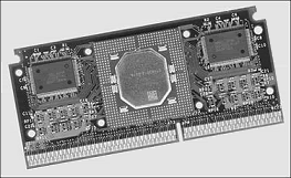
The two variations on these cartridges are called SECC (single edge contact cartridge) and SECC2. Figure 2 shows a diagram of the SECC package; Figure 3 shows the SECC2 package.
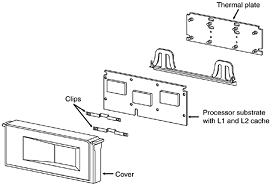
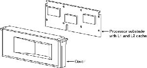
As you can see from these figures, the SECC2 version is cheaper to make because it uses fewer overall parts. It also allows for a more direct heatsink attachment to the processor for better cooling. Intel transitioned from SECC to SECC2 in the beginning of 1999; all later PII chips, and the Slot 1 PIII chips that followed, use the improved SECC2 design.
By using separate chips mounted on a circuit board, Intel could build the Pentium II much less expensively than the multiple die within a package used in the Pentium Pro. Intel could also use cache chips from other manufacturers and more easily vary the amount of cache in future processors compared to the Pentium Pro design.
Intel has offered Pentium II processors with the following speeds:
| CPU Type/Speed | CPU Clock | Motherboard Speed |
|---|---|---|
| Pentium II 233MHz | 3.5x | 66MHz |
| Pentium II 266MHz | 4x | 66MHz |
| Pentium II 300MHz | 4.5x | 66MHz |
| Pentium II 333MHz | 5x | 66MHz |
| Pentium II 350MHz | 3.5x | 100MHz |
| Pentium II 400MHz | 4x | 100MHz |
| Pentium II 450MHz | 4.5x | 100MHz |
The Pentium II processor core has 7.5 million transistors and is based on Intel's advanced P6 architecture. The Pentium II started out using a 0.35-micron process technology, although the 333MHz and faster Pentium IIs are based on 0.25-micron technology.
This enables a smaller die, allowing increased core frequencies and reduced power consumption. At 333MHz, the Pentium II processor delivers a 75%–150% performance boost, compared to the 233MHz Pentium processor with MMX technology, and approximately 50% more performance on multimedia benchmarks.
Aside from speed, the best way to think of the Pentium II is as a Pentium Pro with MMX technology instructions and a slightly modified cache design. It has the same multiprocessor scalability as the Pentium Pro, as well as the integrated L2 cache.
The 57 new multimedia-related instructions carried over from the MMX processors and the capability to process repetitive loop commands more efficiently are included as well. Also included as a part of the MMX upgrade is double the internal L1 cache from the Pentium Pro (from 16KB total to 32KB total in the Pentium II).
Maximum power usage for the Pentium II is shown in the following table:
| Core Speed | Power Draw | Process | Voltage |
|---|---|---|---|
| 450MHz | 27.1w | 0.25-micron | 2.0V |
| 400MHz | 24.3w | 0.25-micron | 2.0V |
| 350MHz | 21.5w | 0.25-micron | 2.0V |
| 333MHz | 23.7w | 0.25-micron | 2.0V |
| 300MHz | 43.0w | 0.35-micron | 2.8V |
| 266MHz | 38.2w | 0.35-micron | 2.8V |
| 233MHz | 34.8w | 0.35-micron | 2.8V |
You can see that the highest speed 450MHz version of the Pentium II actually uses less power than the slowest original 233MHz version! This was accomplished by using the smaller 0.25-micron process and running the processor on a lower voltage of only 2.0V.
Pentium III and subsequent processors used even smaller processes and lower voltages to continue this trend. The Pentium II includes Dynamic Execution, which describes unique performance-enhancing developments by Intel and was first introduced in the Pentium Pro processor.
Major features of Dynamic Execution include multiple branch prediction, which speeds execution by predicting the flow of the program through several branches; dataflow analysis, which analyzes and modifies the program order to execute instructions when ready; and speculative execution, which looks ahead of the program counter and executes instruction that are likely to be needed.
The Pentium II processor expands on these capabilities in sophisticated and powerful new ways to deliver even greater performance gains. Similar to the Pentium Pro, the Pentium II also includes DIB architecture. The term Dual Independent Bus comes from the existence of two independent buses on the Pentium II processor—the L2 cache bus and the processor–to–main-memory system bus.
The Pentium II processor can use both buses simultaneously, thus getting as much as twice as much data in and out of the Pentium II processor as a single-bus architecture processor. The DIB architecture enables the L2 cache of the 333MHz Pentium II processor to run 2 1/2 times as fast as the L2 cache of Pentium processors.
As the frequency of future Pentium II processors increases, so will the speed of the L2 cache. Also, the pipelined system bus enables simultaneous parallel transactions instead of singular sequential transactions. Together, these DIB architecture improvements offer up to three times the bandwidth performance over a single-bus architecture as with the regular Pentium.
The L1 cache always runs at full-core speeds because it is mounted directly on the processor die. The L2 cache in the Pentium II normally runs at half-core speed, which saves money and allows for less expensive cache chips to be used. For example, in a 333MHz Pentium II, the L1 cache runs at a full 333MHz, whereas the L2 cache runs at 167MHz.
Even though the L2 cache is not at full-core speed as it was with the Pentium Pro, this is still far superior to having cache memory on the motherboard running at the 66MHz motherboard speed of most Socket 7 Pentium designs. Intel claims that the DIB architecture in the Pentium II enables up to three times the bandwidth of normal single-bus processors, such as the original Pentium.
By removing the cache from the processor's internal package and using external chips mounted on a substrate and encased in the cartridge design, Intel can now use more cost-effective cache chips and more easily scale the processor up to higher speeds.
The Pentium Pro was limited in speed to 200MHz, largely due to the inability to find affordable cache memory that runs any faster. By running the cache memory at half-core speed, the Pentium II can run up to 400MHz while still using 200MHz-rated cache chips.
To offset the half-core speed cache used in the Pentium II, Intel doubled the basic amount of integrated L2 cache from 256KB standard in the Pro to 512KB standard in the Pentium II. Note that the tag RAM included in the L2 cache enables up to 512MB of main memory to be cacheable in PII processors from 233MHz to 333MHz.
The 350MHz, 400MHz, and faster versions include an enhanced tag-RAM that allows up to 4GB of main memory to be cacheable. This is very important if you ever plan on adding more than 512MB of memory. In that case, you would definitely want the 350MHz or faster version; otherwise, memory performance would suffer.
The system bus of the Pentium II provides "glueless" support for up to two processors. This enables low-cost, two-way multiprocessing on the L2 cache bus. These system buses are designed especially for servers or other mission-critical system use where reliability and data integrity are important.
All Pentium IIs also include parity-protected address/request and response system bus signals with a retry mechanism for high data integrity and reliability. To install the Pentium II in a system, a special processor-retention mechanism is required. This consists of a mechanical support that attaches to the motherboard and secures the Pentium II processor in Slot 1 to prevent shock and vibration damage.
Retention mechanisms should be provided by the motherboard manufacturer. (For example, the Intel Boxed AL440FX and DK440LX motherboards included a retention mechanism, plus other important system integration components.) The Pentium II can generate a significant amount of heat that must be dissipated.
This is accomplished by installing a heatsink on the processor. Many of the Pentium II processors use an active heatsink that incorporates a fan. Unlike heatsink fans for previous Intel boxed processors, the Pentium II fans draw power from a three-pin power header on the motherboard.
Most motherboards provide several fan connectors to supply this power. Special heatsink supports are necessary to furnish mechanical support between the fan heatsink and support holes on the motherboard. Normally, a plastic support is inserted into the heatsink holes in the motherboard next to the CPU, before installing the CPU/heatsink package.
Most fan heatsinks have two components: a fan in a plastic shroud and a metal heatsink. The heatsink is attached to the processor's thermal plate and should not be removed. The fan can be removed and replaced if necessary—for example, if it has failed.
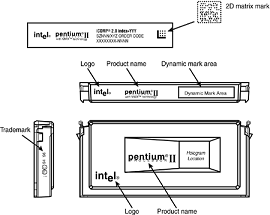
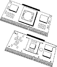
To identify exactly which Pentium II processor you have and what its capabilities are, look at the specification number printed on the SEC cartridge. You will find the specification number in the dynamic mark area on the top of the processor module. See Figure below to locate these markings.
The two variations of the SECC2 cartridge vary by the type of processor core package on the board. The plastic land grid array (PLGA) is the older type of packaging used in previous SECC cartridges and was eventually phased out. A newer organic land grid array (OLGA), which is a processor core package that is smaller and easier to manufacture, took its place.
It also enabled better thermal transfer between the processor die and the heatsink, which was attached directly to the top of the OLGA chip package. Figure below shows the open back side (where the heatsink would be attached) of SECC2 processors with PLGA and OLGA cores.
Pentium II motherboards have an onboard voltage regulator circuit designed to power the CPU. Some Pentium II processors run at several different voltages, so the regulator must be set to supply the correct voltage for the specific processor you are installing.
As with the Pentium Pro and unlike the older Pentium, no jumpers or switches must be set; the voltage setting is handled completely automatically through the VID pins on the processor cartridge. To ensure the system is ready for all Pentium II processor variations, the values in bold must be supported.
Most Pentium II processors run at 2.8V, with some newer ones at 2.0V. The Pentium II Mobile Module is a Pentium II for notebooks that includes the North Bridge of the high-performance 440BX chipset. This is the first chipset on the market that allows 100MHz processor bus operation, although that is currently not supported in the mobile versions.
The 440BX chipset was released at the same time as the 350MHz and 400MHz versions of the Pentium II. Newer variations on the Pentium II include the Pentium IIPE, which is a mobile version that includes 256KB of L2 cache directly integrated into the die. Therefore, it runs at full-core speed, making it faster than the desktop Pentium II because the desktop chips use half-speed L2 cache.


