Processor Bus/Front-Side Bus
The processor bus (also called the front-side bus or FSB) is the communication pathway between the CPU and motherboard chipset, more specifically the North Bridge or Memory Controller Hub.
This bus runs at the full motherboard speed—typically between 66MHz and 800MHz in modern systems, depending on the particular board and chipset design. This same bus also transfers data between the CPU and an external (L2) memory cache on Socket-7 (Pentium class) systems. Figure 1 shows how this bus fits into a typical Socket 7 PC system.
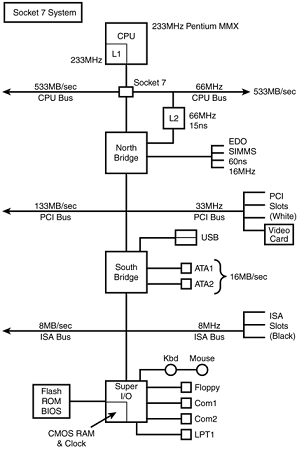
Figure 1 also shows where and how the other main buses, such as the PCI and ISA buses, fit into the system.
As you can see, there is clearly a three-tier architecture with the fastest CPU bus on top, the PCI bus next, and the ISA bus at the bottom. Various components in the system are connected to one of these three main buses.
Socket 7 systems have an external (L2) cache for the CPU; the L2 cache is mounted on the motherboard and connected to the main processor bus that runs at the motherboard speed (usually between 66MHz and 100MHz).
Thus, as the Socket 7 processors became available in faster and faster versions (through increasing the clock multiplier in the chip), the L2 cache unfortunately remained stuck on the motherboard running at the relatively slow (by comparison) motherboard speed.
For example, the fastest Intel Socket 7 systems ran the CPU at 233MHz, which was 3.5x the CPU bus speed of 66MHz. Therefore, the L2 cache ran at only 66MHz.
The fastest Socket 7 systems used the AMD K6-2 550 processor, which ran at 550MHz—5.5x a CPU bus speed of 100MHz. In those systems, the L2 cache ran at only 100MHz.
The problem of the slow L2 cache was first solved in the P6 class processors, such as the Pentium Pro, Pentium II, Celeron, Pentium III, and AMD Athlon and Duron. These processors used either Socket 8, Slot 1, Slot 2, Slot A, Socket A, or Socket 370.
They moved the L2 cache off the motherboard and directly onto the CPU and connected it to the CPU via an on-chip back-side bus. Because the L2 cache bus was called the back-side bus, some in the industry began calling the main CPU bus the front-side bus. I still usually refer to it simply as the CPU bus.
By incorporating the L2 cache into the CPU, it can run at speeds up to the same speed as the processor itself. Most processors now incorporate the L2 cache directly on the CPU die, so the L2 cache runs at the same speed as the rest of the CPU.
Others (mostly older versions) used separate die for the cache integrated into the CPU package, which ran the L2 cache at some lower multiple (one-half, two-fifth, or one-third) of the main CPU. Even if the L2 ran at half or one-third of the processor speed, it still was significantly faster than the motherboard-bound cache on the Socket 7 systems.
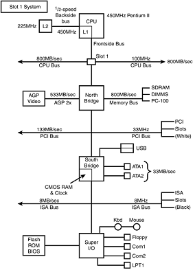 Figure 2 shows a typical Slot-1 type system, in which the L2 cache is built in to the CPU but running at only half the processor speed.
This would also be the same for systems using Slot A. The CPU bus speed increased from 66MHz (used primarily in Socket 7 systems) to 100MHz, enabling a bandwidth of 800MBps.
Note that most of these systems included AGP support. Basic AGP was 66MHz (twice the speed of PCI), but most of these systems incorporated AGP 2x, which operated at twice the speed of standard AGP and enabled a bandwidth of 533 MBps.
These systems also typically used PC-100 SDRAM DIMMs, which have a bandwidth of 800MBps, matching the processor bus bandwidth for the best performance. Slot 1 was dropped in favor of Socket 370 for the Pentium III and Celeron systems.
This was mainly because these newer processors incorporated the L2 cache directly into the CPU die (running at the full-core speed of the processor) and an expensive cartridge with multiple chips was no longer necessary.
At the same time, processor bus speeds increased to 133MHz, which enabled a throughput of 1,066MBps.
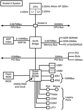 Figure 3 shows a typical Socket 370 system design. AGP speed was also increased to AGP 4x, with a bandwidth of 1,066MBps.
Note the use of what Intel calls "hub architecture" instead of the older North/South Bridge design.
This moves the main connection between the chipset components to a separate 266MBps hub interface (which has twice the throughput of PCI) and enables PCI devices to use the full bandwidth of PCI without fighting for bandwidth with a South Bridge.
Also note that the flash ROM BIOS chip is now referred to as a Firmware Hub and is connected to the system via the LPC bus instead of via the Super I/O chip as in older North/South Bridge designs.
The ISA bus is no longer used in most of these systems, and the Super I/O is connected via the LPC bus instead of ISA. The Super I/O chip also can easily be eliminated in these designs.
This is commonly referred to as a legacy-free system because the ports supplied by the Super I/O chip are now known as legacy ports.
Devices that would have used legacy ports must then be connected to the system via USB instead, and such systems would feature two USB controllers, with up to four total ports (more can be added by attaching USB hubs). AMD processor systems adopted a Socket A design, which is similar to Socket 370 except it uses faster processor and memory buses.
Although early versions retained the older North/South Bridge design, more recent versions use a design similar to Intel's hub architecture. Note the high-speed CPU bus running up to 333MHz (2,664MBps throughput) and the use of DDR SDRAM DIMM modules that support a matching bandwidth of 2,664MBps.
It is always best for performance when the bandwidth of memory matches that of the processor. Finally, note how most of the South Bridge components include functions otherwise found in Super I/O chips; when these functions are included the chip is called a Super South Bridge.
The Pentium 4 uses a Socket 423 or Socket 478 design with hub architecture.
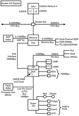
This design is most notable for including a 400MHz, 533MHz, or 800MHz CPU bus with a bandwidth of 3,200MBps, 4,266MBps, or 6,400MBps.
The 533MHz and 800MHz models are currently faster than anything else on the market. In this example, note the use of dual-channel PC3200 (DDR400) SDRAM.
A single PC-3200 DIMM has a bandwidth of 3,200MBps, but when running dual-channel (identical pairs of memory) memory, it has a bandwidth of 6,400MBps—which matches the bandwidth of the 800MHz CPU bus models of the Pentium 4 for best performance.
Processors with the 533MHz CPU bus can use pairs of PC2100 (DDR266) or PC2700 (DDR333) memory modules in dual channel mode to match the 4,266MBps throughput of this memory bus.
It is always best when the throughput of the memory bus matches that of the processor bus.
Because the purpose of the processor bus is to get information to and from the CPU at the fastest possible speed, this bus typically operates at a rate faster than any other bus in the system.
The bus consists of electrical circuits for data, addresses, and control purposes. Most processors since the original Pentium have a 64-bit data bus, so they transfer 64 bits (8 bytes) at a time over the CPU bus. The processor bus operates at the same base clock rate as the CPU does externally.
This can be misleading because most CPUs these days run at a higher clock rate internally than they do externally. For example, an AMD Athlon 3200+ system has a processor running at 2.2GHz internally but only 333MHz externally, whereas a Pentium 4 3.2GHz runs at 3.2GHz internally but only 800MHz externally.
In newer systems, the actual processor speed is some multiple (2x, 2.5x, 3x, and higher) of the processor bus. The processor bus is tied to the external processor pin connections and can transfer 1 bit of data per data line every cycle. Most modern processors transfer 64 bits (8 bytes) of data at a time.
To determine the transfer rate for the processor bus, you multiply the data width (64 bits or 8 bytes for a Celeron/Pentium III/4 or Athlon/Duron/Athlon XP) by the clock speed of the bus (the same as the base or unmultiplied clock speed of the CPU).
For example, if you are using a Pentium 4 3.6GHz processor that runs on an 800MHz processor bus, you have a maximum instantaneous transfer rate of roughly 6,400MBps. You get this result by using the following formula:
800MHz x 8 bytes (64 bits) = 6,400MBps
With slower versions of the Pentium 4, you get either
533.33MHz x 8 bytes (64 bits) = 4,266MBps
or
400MHz x 8 bytes (64 bits) = 3,200MBps
With Socket A (Athlon XP), you get
333.33MHz x 8 bytes (64 bits) = 2,667MBps
or
266.66MHz x 8 bytes (64 bits) = 2,133MBps
or
200MHz x 8 bytes (64 bits) = 1,600MBps
With Socket 370 (Pentium III), you get
133.33MHz x 8 bytes (64 bits) = 1,066MBps
or
100MHz x 8 bytes (64 bits) = 800MBps
This transfer rate, often called the bandwidth of the processor bus, represents the maximum speed at which data can move.


