Processor Manufacturing
Processors are manufactured primarily from silicon, the second most common element on the planet (only the element oxygen is more common). Silicon is the primary ingredient in beach sand; however, in that form it isn't pure enough to be used in chips.
The manner in which silicon is formed into chips is a lengthy process that starts by growing pure silicon crystals via what is called the Czochralski method (named after the inventor of the process). In this method, electric arc furnaces transform the raw materials (primarily quartz rock that is mined) into metallurgical-grade silicon.
Then to further weed out impurities, the silicon is converted to a liquid, distilled, and then redeposited in the form of semiconductor-grade rods, which are 99.999999% pure. These rods are then mechanically broken up into chunks and packed into quartz crucibles, which are loaded into electric crystal pulling ovens.
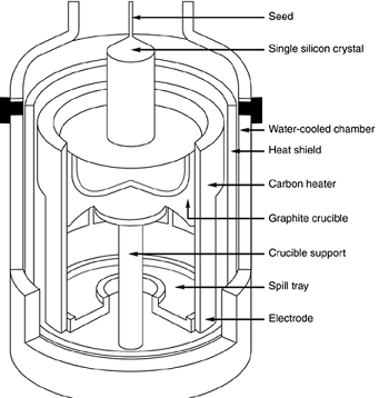
There the silicon chunks are melted at more than 2,500° Fahrenheit. To prevent impurities, the ovens usually are mounted on very thick concrete cubes—often on a suspension to prevent any vibration, which would damage the crystal as it forms.
After the silicon is melted, a small seed crystal is inserted into the molten silicon and slowly rotated. As the seed is pulled out of the molten silicon, some of the silicon sticks to the seed and hardens in the same crystal structure as the seed.
By carefully controlling the pulling speed (10–40 millimeters per hour) and temperature (approximately 2,500°F), the crystal grows with a narrow neck that then widens into the full desired diameter. Depending on the chips being made, each ingot is 200mm (approximately 8'') or 300mm (12'') in diameter and more than 5 feet long, weighing hundreds of pounds.
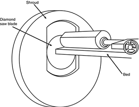
The ingot is then ground into a perfect 200mm- (8'') or 300mm-diameter (12'') cylinder, with a small, flat cut on one side for positioning accuracy and handling. Each ingot is then cut with a high-precision diamond saw into more than a thousand circular wafers, each less than a millimeter thick. Each wafer is then polished to a mirror-smooth surface.
Chips are manufactured from the wafers using a process called photolithography. Through this photographic process, transistors and circuit and signal pathways are created in semiconductors by depositing different layers of various materials on the chip, one after the other. Where two specific circuits intersect, a transistor or switch can be formed.
The photolithographic process starts when an insulating layer of silicon dioxide is grown on the wafer through a vapor deposition process. Then a coating of photoresist material is applied, and an image of that layer of the chip is projected through a mask onto the now light-sensitive surface.
Doping is the term used to describe chemical impurities added to silicon (which is naturally a non conductor), creating a material with semiconductor properties. The projector uses a specially created mask, which is essentially a negative of that layer of the chip etched in chrome on a quartz plate.
Modern processors have 20 or more layers of material deposited and partially etched away (each requiring a mask) and up to six or more layers of metal interconnects. As the light passes through a mask, the light is focused on the wafer surface, exposing the photoresist with the image of that layer of the chip.
Each individual chip image is called a die. A device called a stepper then moves the wafer over a little bit, and the same mask is used to imprint another chip die immediately next to the previous one.
After the entire wafer is imprinted with a layer of material and photoresist, a caustic solution washes away the areas where the light struck the photoresist, leaving the mask imprints of the individual chip circuit elements and pathways.
Then, another layer of semiconductor material is deposited on the wafer with more photoresist on top, and the next mask is used to expose and then etch the next layer of circuitry. Using this method, the layers and components of each chip are built one on top of the other until the chips are completed.
Some of the masks are used to add the metallization layers, which are the metal interconnects used to tie all the individual transistors and other components together. Most chips use aluminum interconnects, although during 2002 many moved to copper.
The first commercial PC processor chip to use copper was the 0.18-micron Athlon made in AMD's Dresden fab, and Intel has shifted the Pentium 4 to copper with the 0.13-micron Northwood version.
Copper is a better conductor than aluminum and allows smaller interconnects with less resistance, meaning smaller and faster chips can be made.
The reason copper hadn't been used until recently is that there were difficult corrosion problems to overcome during the manufacturing process that were not as much of a problem with aluminum. Now that these problems have been solved, more and more chips will be fabricated with copper interconnects.
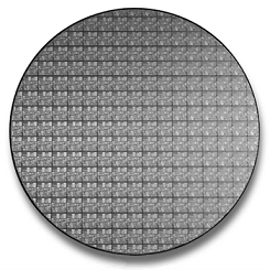
A completed circular wafer has as many chips imprinted on it as can possibly fit. Because each chip usually is square or rectangular, there are some unused portions at the edges of the wafer, but every attempt is made to use every square millimeter of surface.
The industry is going through several transitions in chip manufacturing. The trend in the industry is to use both larger wafers and a smaller chip die process. Process refers to the size and spacing of the individual circuits and transistors on the chip.
In late 2001 and into 2002, chip manufacturing processes began moving from the 0.18-micron to the 0.13-micron process, the metal interconnects on the die began moving from aluminum to copper, and wafers began moving from 200mm (8'') to 300mm (12'') in diameter.
The larger 300mm wafers alone enable more than double the number of chips to be made, compared to the 200mm used previously. The smaller 0.13-micron process enables more transistors to be incorporated into the die while maintaining a reasonable die size and allowing for a sufficient yield.
This means the trend for incorporating more and more cache within the die will continue, and transistor counts will rise to 1 billion per chip or more by 2007. As an example of how this can affect a particular chip, let's look at the Pentium 4. The standard wafer size used in the industry for many years was 200mm in diameter, or just under 8''.
This results in a wafer of about 31,416 square millimeters in area. The first version of the Pentium 4 with the Willamette core used a 0.18-micron process with aluminum interconnects on a die that was 217 square millimeters in area, had 42 million transistors, and was made on 200mm wafers.
Therefore, up to 145 of these chips could fit on a 200mm (8'') wafer. The newer Pentium 4 processors with the Northwood core use a smaller 0.13-micron process with copper interconnects on a die that is 131 square millimeters in area with 55 million transistors.
Northwood has double the on-die L2 cache (512KB) as compared to Willamette, which is why the transistor count is significantly higher. Even with the higher transistor count, the smaller 0.13-micron process results in a die that is more than 60% smaller, allowing up to 240 chips to fit on the same 200mm (8'') wafer that could hold only 145 Willamette die.
Starting in early 2002, Intel began producing Northwood on the larger 300mm wafers, which have a surface area of 70,686 square millimeters. These wafers have 2.25 times the surface area of the smaller 200mm wafers, enabling more than double the number of chips to be produced per wafer.
In the case of the Pentium 4 Northwood, up to 540 chip dies fit on a 300mm wafer. By combining the smaller die with the larger wafer, Pentium 4 production has increased by more than 3.7 times since the chip was first introduced. This is one reason newer chips are often more plentiful and less expensive than older ones.
The next transition in the industry will be to a 0.09-micron process sometime in 2003, a 0.065-micron process in 2005, and a 0.045 process in 2007. These advancements in process will allow 1 billion transistors per chip in 2007!
All these will still be made on 300mm wafers because the next wafer transition isn't expected until 2015, when a transition to 450mm wafers is being considered. Table below lists the CPU process transitions.
| Date: | 1989 | 1991 | 1993 | 1995 | 1997 | 1999 | 2001 | 2003 | 2005 | 2007 | 2009 |
| Process: | 1.0 | 0.8 | 0.5 | 0.35 | 0.25 | 0.18 | 0.13 | 0.09 | 0.065 | 0.045 | 0.032 |
Note that not all the chips on each wafer will be good, especially as a new production line starts. As the manufacturing process for a given chip or production line is perfected, more and more of the chips will be good. The ratio of good to bad chips on a wafer is called the yield.
Yields well under 50% are common when a new chip starts production; however, by the end of a given chip's life, the yields are normally in the 90% range. Most chip manufacturers guard their yield figures and are very secretive about them because knowledge of yield problems can give their competitors an edge.
A low yield causes problems both in the cost per chip and in delivery delays to their customers. If a company has specific knowledge of competitors' improving yields, it can set prices or schedule production to get higher market share at a critical point.
After a wafer is complete, a special fixture tests each of the chips on the wafer and marks the bad ones to be separated out later. The chips are then cut from the wafer using either a high-powered laser or diamond saw. After being cut from the wafers, the individual dies are then retested, packaged, and retested again.
The packaging process is also referred to as bonding because the die is placed into a chip housing in which a special machine bonds fine gold wires between the die and the pins on the chip. The package is the container for the chip die, and it essentially seals it from the environment.
After the chips are bonded and packaged, final testing is done to determine both proper function and rated speed. Different chips in the same batch often run at different speeds. Special test fixtures run each chip at different pressures, temperatures, and speeds, looking for the point at which the chip stops working.
At this point, the maximum successful speed is noted and the final chips are sorted into bins with those that tested at a similar speed. For example, the Pentium 4 2.0A, 2.2, 2.26, 2.4, and 2.53GHz are all exactly the same chip made using the same die. They were sorted at the end of the manufacturing cycle by speed.
One interesting thing about this is that as a manufacturer gains more experience and perfects a particular chip assembly line, the yield of the higher-speed versions goes way up. So, of all the chips produced from a single wafer, perhaps more than 75% of them check out at the highest speed and only 25% or less run at the lower speeds.
The paradox is that Intel often sells a lot more of the lower-priced, lower-speed chips, so it just dips into the bin of faster ones, labels them as slower chips, and sells them that way. People began discovering that many of the lower-rated chips actually ran at speeds much higher than they were rated, and the business of overclocking was born.

