Third-Generation Processors
The third generation represents perhaps the most significant change in processors since the first PC. The big deal was the migration from processors that handled 16-bit operations to true 32-bit chips.
The third-generation processors were so far ahead of their time, it took fully 10 years before 32-bit operating systems and software became mainstream, and by that time the third-generation chips had become a memory. The following section details the third-generation processors.
386 Processors
The Intel 80386 (usually abbreviated as 386) caused quite a stir in the PC industry because of the vastly improved performance it brought to the personal computer. Compared with 8088 and 286 systems, the 386 chip offered greater performance in almost all areas of operation.
The 386 is a full 32-bit processor optimized for high-speed operation and multitasking operating systems. Intel introduced the chip in 1985, but the 386 appeared in the first systems in late 1986 and early 1987. The Compaq Deskpro 386 and systems made by several other manufacturers introduced the chip; somewhat later, IBM used the chip in its PS/2 Model 80.
The 386 can execute the real-mode instructions of an 8086 or 8088, but in fewer clock cycles. The 386 was as efficient as the 286 in executing instructions—the average instruction took about 4.5 clock cycles. In raw performance, therefore, the 286 and 386 actually seemed to be at almost equal clock rates.
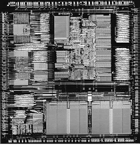
The 386 offered greater performance in other ways, mainly because of additional software capability (modes) and a greatly enhanced memory management unit (MMU). The die for the 386 is shown in Figure below.
The 386 can switch to and from protected mode under software control without a system reset—a capability that makes using protected mode more practical. In addition, the 386 includes a new mode, called virtual real mode, which enables several real-mode sessions to run simultaneously under protected mode.
The protected mode of the 386 is fully compatible with the protected mode of the 286. The protected mode for both chips often is called their native mode of operation because these chips are designed for advanced operating systems such as Windows NT/2000/XP, which run only in protected mode.
Intel extended the memory-addressing capabilities of 386 protected mode with a new MMU that provided advanced memory paging and program switching. These features were extensions of the 286 type of MMU, so the 386 remained fully compatible with the 286 at the system-code level.
The 386 chip's virtual real mode was also new. In virtual real mode, the processor could run with hardware memory protection while simulating an 8086's real-mode operation. Multiple copies of DOS and other operating systems, therefore, could run simultaneously on this processor, each in a protected area of memory.
If the programs in one segment crashed, the rest of the system was protected. Numerous variations of the 386 chip exist, some of which are less powerful and some of which are less power hungry. The following sections cover the members of the 386-chip family and their differences.
386DX Processors
The 386DX chip was the first of the 386 family members that Intel introduced. The 386 is a full 32-bit processor with 32-bit internal registers, a 32-bit internal data bus, and a 32-bit external data bus. The 386 contains 275,000 transistors in a very large scale integration (VLSI) circuit.
The chip comes in a 132-pin package and draws approximately 400 milliamperes (ma), which is less power than even the 8086 requires. The 386 has a smaller power requirement because it is made of Complementary Metal-Oxide Semiconductor (CMOS) materials.
The CMOS design enables devices to consume extremely low levels of power. The Intel 386 chip was available in clock speeds ranging from 16MHz–33MHz; other manufacturers, primarily AMD and Cyrix, offered comparable versions with speeds up to 40MHz.
The 386DX can address 4GB of physical memory. Its built-in virtual memory manager enables software designed to take advantage of enormous amounts of memory to act as though a system has 64TB of memory. (A terabyte, or TB, is 1,099,511,627,776 bytes of memory, or about 1,000GB.)
386SX Processors
The 386SX was designed for systems designers looking for 386 capabilities at 286 system prices. Similar to the 286, the 386SX is restricted to only 16 bits when communicating with other system components, such as memory. Internally, however, the 386SX is identical to the DX chip; the 386SX has 32-bit internal registers and can therefore run 32-bit software.
The 386SX uses a 24-bit memory-addressing scheme like that of the 286, rather than the full 32-bit memory address bus of the standard 386. The 386SX, therefore, can address a maximum 16MB of physical memory rather than the 4GB of physical memory the 386DX can address.
Before it was discontinued, the 386SX was available in clock speeds ranging from 16MHz to 33MHz. The 386SX signaled the end of the 286 because of the 386SX chip's superior MMU and the addition of the virtual real mode. Under a software manager such as Windows or OS/2, the 386SX can run numerous DOS programs at the same time.
The capability to run 386-specific software is another important advantage of the 386SX over any 286 or older design. For example, Windows 3.1 runs nearly as well on a 386SX as it does on a 386DX.
386SL Processors
The 386SL is another variation on the 386 chip. This low-power CPU had the same capabilities as the 386SX, but it was designed for laptop systems in which low power consumption was necessary. The SL chips offered special power-management features that were important to systems that ran on batteries. The SL chip also offered several sleep modes to conserve power.
The chip included an extended architecture that contained a System Management Interrupt (SMI), which provided access to the power-management features. Also included in the SL chip was special support for LIM (Lotus Intel Microsoft) expanded memory functions and a cache controller.
The cache controller was designed to control a 16KB–64KB external processor cache. These extra functions account for the higher transistor count in the SL chips (855,000) compared with even the 386DX processor (275,000). The 386SL was available in 25MHz clock speed.
Intel offered a companion to the 386SL chip for laptops called the 82360SL I/O subsystem. The 82360SL provided many common peripheral functions, such as serial and parallel ports, a direct memory access (DMA) controller, an interrupt controller, and power-management logic for the 386SL processor.
This chip subsystem worked with the processor to provide an ideal solution for the small size and low power-consumption requirements of portable and laptop systems.
80387 Coprocessor
Although the 80387 chips ran asynchronously, 386 systems were designed so that the math chip ran at the same clock speed as the main CPU. Unlike the 80287 coprocessor, which was merely an 8087 with different pins to plug into the AT motherboard, the 80387 coprocessor was a high-performance math chip specifically designed to work with the 386.
All 387 chips used a low power-consumption CMOS design. The 387 coprocessor had two basic designs: the 387DX coprocessor, which was designed to work with the 386DX processor, and the 387SX coprocessor, which was designed to work with the 386SX, SL, or SLC processor.
Intel originally offered several speeds for the 387DX coprocessor. But when the company designed the 33MHz version, a smaller mask was required to reduce the lengths of the signal pathways in the chip. This increased the performance of the chip by roughly 20%.

